>/posts/Sword Of Secrets - 0x0 Overview $
Estimated reading time: 6 minutes

What's that?
Because I need to practice my skills in IoT and physical security of electronic devices, I decided to buy the Sword of Secrets hardware crypto CTF kit, which recently arrived. If you don't know what that is, don't worry you haven't missed anything important. In this post I'll explain how it works, what it's used for, how to work with it, and what it actually is. You can read the project details here: Sword of secrets
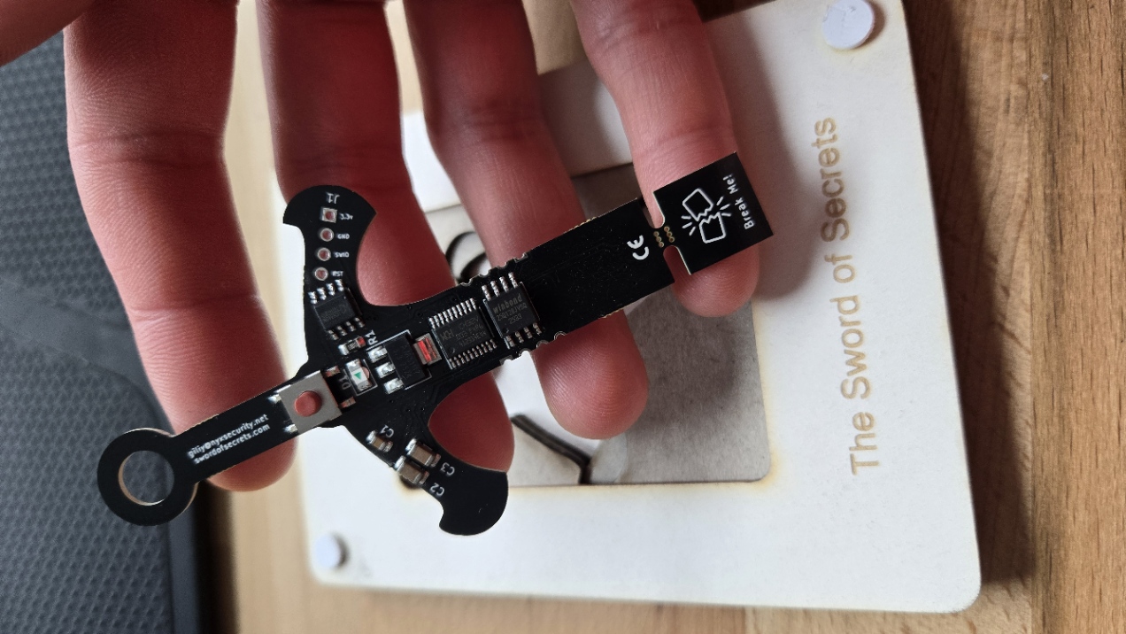
The sword is well made, and the PCB contains only the minimum amount of electronics required for it to function properly. In front of the USB pads, there is a small section of the PCB without traces labeled "Break Me." Snap it off, but don't throw it away, you'll need it in a moment. Insert the broken-off piece into the USB port first, and then slide in the main PCB so that the pads align with the port. Without the snapped fragment, the sword doesn't make proper contact, which is why the broken piece acts as a necessary spacer. After plugging it in, the green LED on the board blinks a few times, and then the sword stops performing any further actions. No external drivers are required as it works out of the box.
What's on a board?
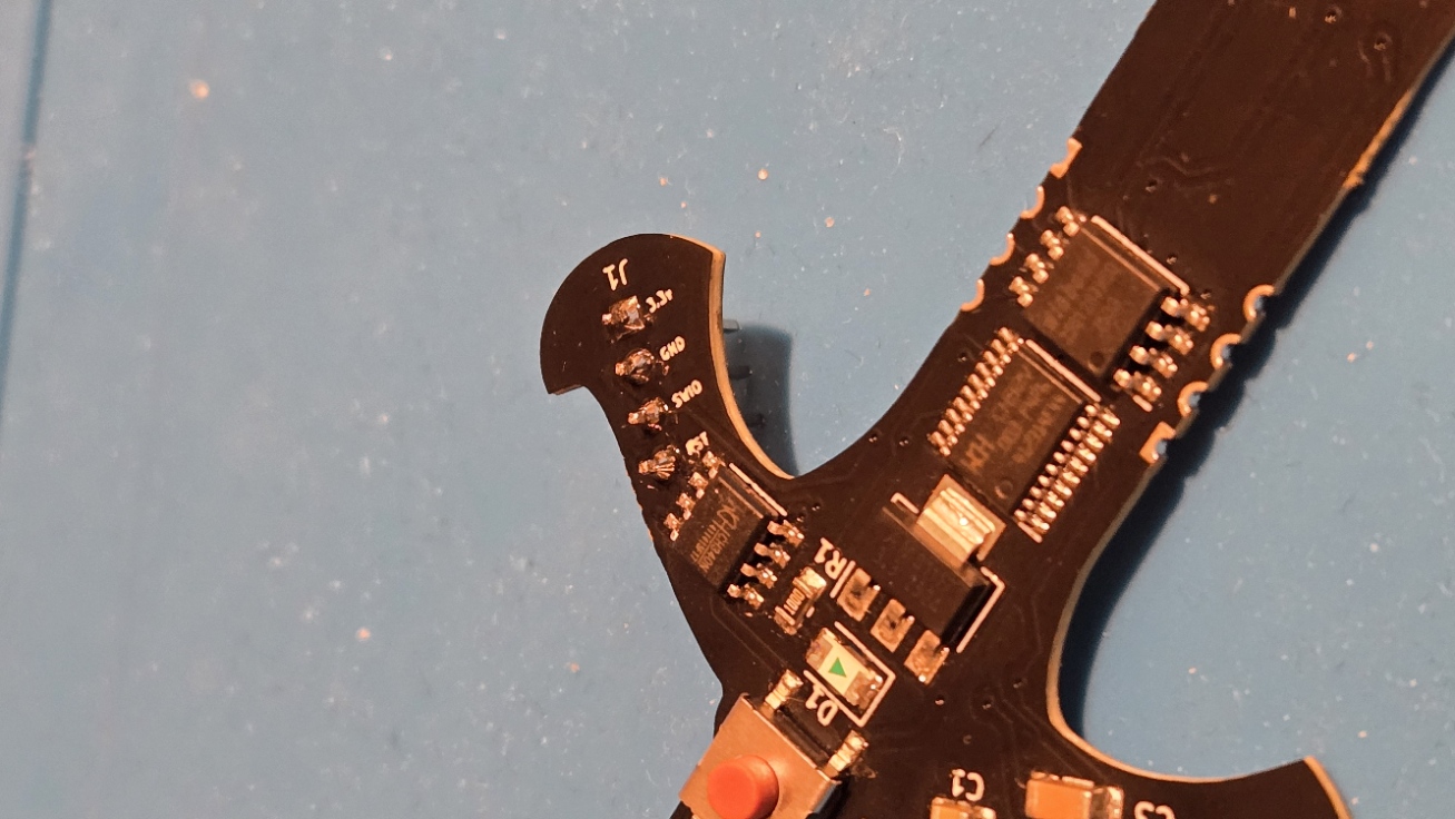
The board includes a 3V3 linear voltage regulator, and this voltage is supplied to all components on the PCB. The logic level is also 3V, so be careful not to accidentally connect boards that operate at 5V logic or make sure to use a proper logic level shifter. Besides the LDO, the board features a USB -> UART converter, a NOR Flash memory chip, the main microcontroller, and pads for connecting a debugger. The documentation for all the components can be downloaded from the project’s GitHub repository: GitHub
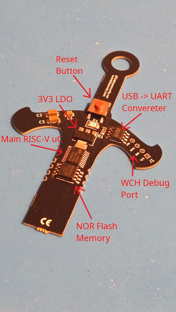
I soldered header pins for debugging immediately after unboxing it, although I haven't used them yet. In its default configuration, the chip has debugging access locked. Well ulocking it will be another exercise once I finish the crypto challenges. The minimal design also makes it perfect for testing future side-channel and fault injection attacks.
How does it works?
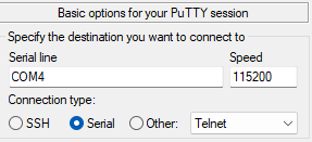
After being connected, the device waits briefly for a new firmware upload. If nothing happens during that time, it proceeds to initialize the UART interface and enter the main loop, where its tasks are executed. To communicate with it, we first need to determine the device's COM port number. We can do this through the Device Manager.
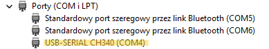
In my screenshot, you can see that it appears as COM4. To connect to the device, we also need to know the baud rate it uses. Most commonly, this will be either 9600 or 115200. The configuration code available in the CTF repository suggests that the correct value is 115200, so that's the one we'll use.
Fortunately, entering the wrong baud rate won't cause any damage the only effect is that you might see garbled characters and other non-printable symbols on the screen instead of readable output. There's nothing stopping you from simply testing all common speeds. If you'd like to learn how to empirically determine a UART baud rate, let me know in the comments I'd be happy to cover that as well. So here's my PuTTy config:
As you might see the device is not very communicative...
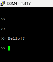
But don't worry, don't close PuTTy and click reset button.
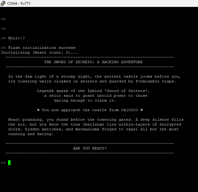
The welcome message is displayed only once during startup, so by the time we finish setting everything up, it's already gone.
How to talk to it?!
The device responds with silence to everything we send but after reviewing the documentation, you'll notice that there are actually a few commands it does respond to:
SOLVE - Starts the challenge verification sequence
ASSERT - Pulls the external flash CS (Chip Select) line low — manual SPI control
RELEASE - Pulls the CS line high
BEGIN - Initializes SPI
END - Terminates SPI
DATA <hex bytes> - Sends raw bytes over SPI and prints the response
RESET - Resets the challenge data on the external flash (calls setupQuest())
REBOOT - Restarts the MCU
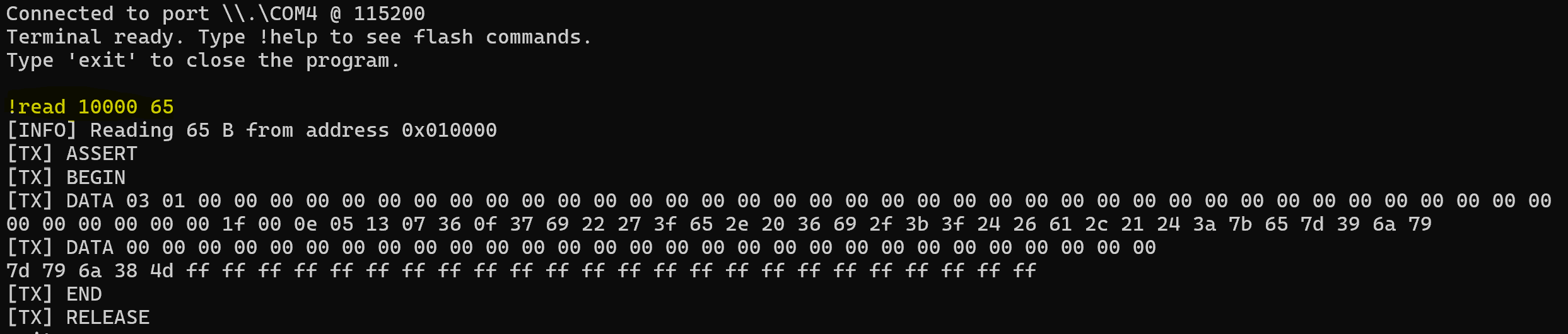
In the previous section, you may have noticed that the first challenge is located at address 0x10000 so let's read what's stored there.We need to pass to the DATA command 0x03 and then address in memory 0x1000 and 65 zero-bytes that will be OR-ed with bytes from flash memory.
> ASSERT
> BEGIN
> DATA 03 01 00 00 00 00 00 00 00 00 00 00 00 00 00 00 00 00 00 00 00 00 00 00 00 00 00 00 00 00 00 00 00 00 00 00 00 00 00 00
> DATA 00 00 00 00 00 00 00 00 00 00 00 00 00 00 00 00 00 00 00 00 00 00 00 00 00 00 00 00 00
> RELEASE
> END
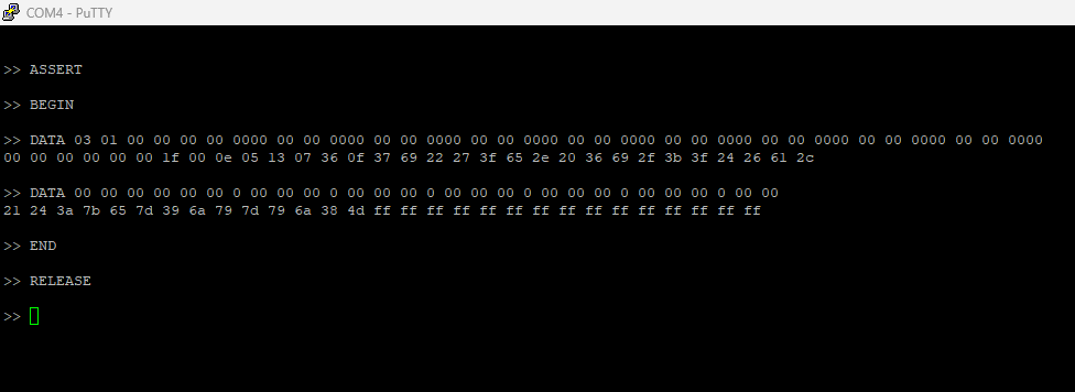
As you can see, typing commands like this is slightly inefficient, so I wrote a pseudo-terminal to automate the process with a set of simplified commands.
So what's the challenge here?
Since bytes with the value 0xFF indicate uninitialized (erased) flash memory, I copied everything up to the point where they begin and the bytes here we've read are challenge itself:
00 00 00 00 0e 05 13 07 36 0f 37 69 22 27 3f 65 2e 20 36 69 2f 3b 3f 24 26 61 2c 21 24 3a 7b 65 7d 39 6a 79 7d 79 6a 38 4d
If you're not sure what this is about don't worry. We'll cover it in the next post in this series!
Bartosz Osuch
X
Comments (0)
Please log in to add a comment.